
Writing LUT level design
Published:
The pre-requisites required for this blog are Digital VLSI Design, RTL Design using Verilog and FPGA structure the knowledge of CLBs and Slices. Many a time it is required to write a LUT level design for a better overview of the design space exploration and also to get better control for design such as ring oscillators etc.
In this blog, I will focus mostly on the details of How do we write LUT based code instead of simple Verilog syntax in the same file. It is assumed that the reader is aware of Verilog and other digital design concepts.
Let’s look at the Lookup Table LUT design at the gate level, LUT is a basic block of a FPGA, as the name suggests LUTs looks for a table, the table here is the function output in a truth table representation, i.e when you write an expanded truth table the column corresponding to the function is what we are talking about. Now there is a nice White Paper by Altera, for more details have a look. A LUT-6 from two LUT-3 looks like this
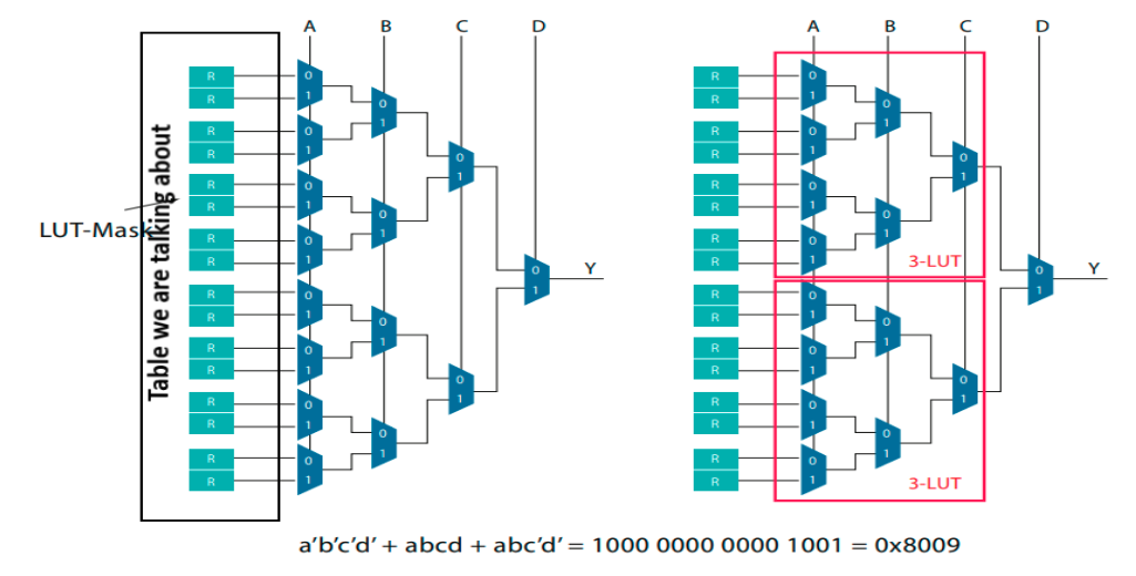
Fig: LUT-6 from two LUT-3, Altera FPGA Architecture White Paper.
How do we instantiate LUTs directly in verilog scripts?
The code snippet is taken from the Vivado Design Suite 7 Series FPGA Libraries Guide
Verilog Instantiation Template
// LUT6: 6-input Look-Up Table with general output
// 7 Series
// Xilinx HDL Libraries Guide, version 2012.2
LUT6 #(
.INIT(64'h0000000000000000) // Specify LUT Contents
) LUT6_inst (
.O(O), // LUT general output
.I0(I0), // LUT input
.I1(I1), // LUT input
.I2(I2), // LUT input
.I3(I3), // LUT input
.I4(I4), // LUT input
.I5(I5) // LUT input
);
// End of LUT6_inst instantiation
Fig:- This code snippet is taken from the Vivado Design Suit 7 Series FPGA
.INIT() stores the truth table of the 6 input logic function, with LSB on the left
LUT6_inst needs to be changed for all the different instantiation done
.I”x” are the inputs with x from 0 to 5 as 6 inputs with I0 as LSB
.O is the output of the LUT.
2-Input NAND gate example
In Verilog, in RTL we write
y=~(a&b)
Its translation to a LUT design would be
Verilog Instantiation Template
// LUT6: 6-input Look-Up Table with general output
// 7 Series
// Xilinx HDL Libraries Guide, version 2012.2
LUT6 #(
.INIT(64'h0000000000000007) // Specify LUT Contents
) LUT6_inst (
.O(y), // LUT general output
.I0(a), // LUT input
.I1(b), // LUT input
.I2(0), // LUT input
.I3(0), // LUT input
.I4(0), // LUT input
.I5(0) // LUT input
);
// End of LUT6_inst instantiation
Output of NAND with inputs as <(1,1), (1,0), (0,1), (0,0)> is <0, 1 , 1, 1> which is 7(4’b0111) in hexadecimal. That is written in the .INIT() considering the LSB and MSB ordering.
Inputs a and b are the I0 and I1 inputs of the LUT remaining inputs of the LUT are set to 0 as we don’t need them, y is the output written in .O().
So using one LUT6 we can realise any 6-input or less 1 output boolean functions. Keep in mind one LUT has only one output.
Additional Information
Some of the design specification desires for the appropriate locations of these LUTs consider a PUF design. The location can be set using LOC constraint by setting Slices(LUTs are present inside the Slices) locations in the constraint file.
Leave a Comment